Next: Description of Mesh Experiments Up: CCD Subpixel Structure Previous: CCD Subpixel Structure
![]()
![]()
![]()
![]()
Next: Description of Mesh Experiments
Up: CCD Subpixel Structure
Previous: CCD Subpixel Structure
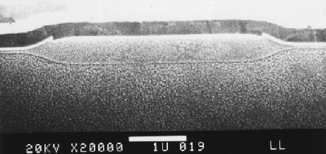
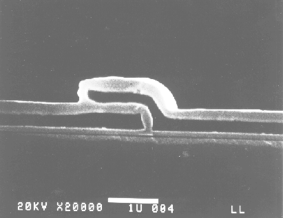
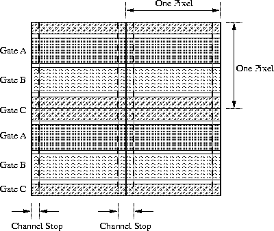
The embedded channel stops run perpendicular to and lie beneath the gates. These structures help confine the charge clouds created by a photoelectric absorption and define the horizontal boundaries of a pixel. Figure 4.34 is a picture of a 2x2 array of pixels and shows the orientation of the gates and channel stops to one another. To fabricate the channel stops, a portion of the insulating Si3N4 layer is etched away. A P+ dopant is then implanted into the bulk silicon. Finally, the silicon is oxidized creating an insulating layer of SiO2 between the channel stop and the gate structure. The gate structure is then grown on top of the silicon after this process. Figure 4.35 is a SEM measurement of a channel stop. The black and white bands at the top of the image are the polysilicon gates and insulating oxide, respectively. The elongated, hexagonal structure is the SiO2 insulator between the P+ channel (not visible in this image) and the gates. The thin white structure between the gates and hexagonal insulator is the Si3N4.
 |
 |
When modeling the quantum efficiency of an ACIS CCD, the complicated gate
structure can
accurately be approximated as uniform slabs of material that cover the
entire CCD. This model
assumes that the charge created by a photon interaction in one of these layers
is not collected by the device (i.e. the layer is ``dead''). This model-The Slab and Stop model-was first
developed by Keith Gendreau during calibration of the ASCA SIS CCDs [Gendreau1995].
The Stop part of the model refers to treating the
hexagonal insulator structure and implanted P+
as rectangular regions of dead SiO2 and Si, respectively.
The absolute calibration of the reference standards involves
fitting the data obtained at the BESSY facility with the Slab and Stop
Model. While the BESSY measurements determine the thicknesses of the gate
slabs, they prove insufficient for constraining the channel stop
parameters![]() .
Construction of a highly accurate CCD model, then, requires determination
of this information in some other fashion.
.
Construction of a highly accurate CCD model, then, requires determination
of this information in some other fashion.
Mark Bautz