


The ACIS team has conducted an extensive calibration program (see, for example, the poster by Pivovaroff et al). To assess the impact of residual calibration errors on ACIS measurements, we have simulated several representative observations. We report the expected magnitude calibration-related errors in source model parameters.
Figure 1
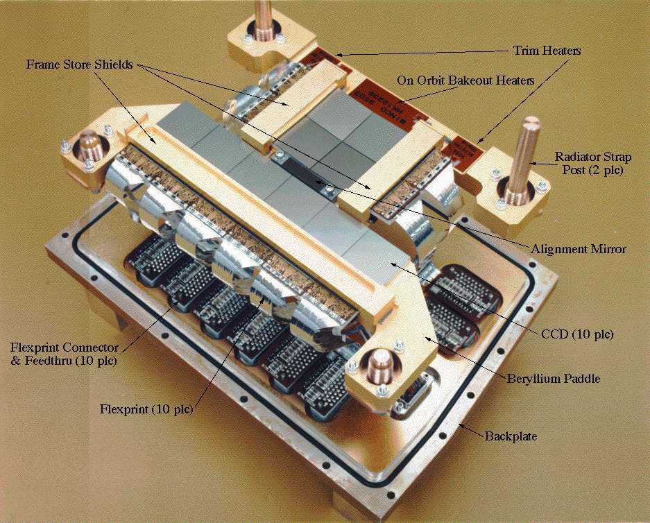
Figure 1: The ACIS flight focal plane, which consists of 8
front-illuminated and 2 back-illuminated MIT Lincoln Laboratory CCID17
detectors. Each detector contains 1024 x 1026 pixels, and each pixel
measures 24 x 24  m. Thus each detector measures about 1 inch
square. The four imaging detectors, arranged in a square, are tilted
to approximate the AXAF High-Resolution Mirror Assembly's focal
surface. The field of view of the imaging detectors is 17 arcmin on
each side. The six detectors in the linear array conform to the
Rowland circle of the AXAF High-Energy Transmission Gratings, and can
be used for grating spectroscopy or imaging. The back-illuminated
detectors are the second and fourth from the left in the spectroscopy
array.
m. Thus each detector measures about 1 inch
square. The four imaging detectors, arranged in a square, are tilted
to approximate the AXAF High-Resolution Mirror Assembly's focal
surface. The field of view of the imaging detectors is 17 arcmin on
each side. The six detectors in the linear array conform to the
Rowland circle of the AXAF High-Energy Transmission Gratings, and can
be used for grating spectroscopy or imaging. The back-illuminated
detectors are the second and fourth from the left in the spectroscopy
array.

Figure 2: An ASCA SIS focal plane detector. Each of the two SIS
sensors contains a focal plane like the one shown here, comprised of 4
front-illuminated MIT Lincoln Laboratory CCID7 detectors. Each
detector contains 420 x 422 pixels, and each pixel measures 27 x 27
 m. Thus each CCD detector measures about 1/2 inch square. The
field of view at the ASCA focal plane is about 22 arcmin square.
m. Thus each CCD detector measures about 1/2 inch square. The
field of view at the ASCA focal plane is about 22 arcmin square.
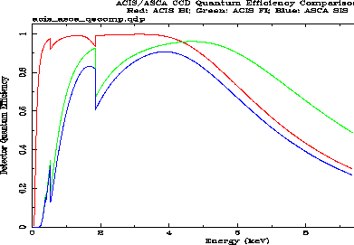
Figure 3: Comparsion of ACIS and ASCA SIS Detector Quantum Efficiencies.
All curves are derived from ground calibration data. The ASCA data
were obtained by Gendreau (MIT PhD Thesis, 1995). ACIS detectors
shown in red (Back-illuminated detector; BI) and green
(Front-illuminated detector; FI) and the ASCA SIS detector in blue.
The ACIS curves are for ASCA grades 0,2,3,4 and 6, with split-event
threshold (spt) of 15 e ; the ASCA SIS curve is for grades 0,2,3
and 4, for spt = 40 e
; the ASCA SIS curve is for grades 0,2,3
and 4, for spt = 40 e . Both curves represent pre-launch
performance.
. Both curves represent pre-launch
performance.
Why do ACIS detectors have higher quantum efficiency?
 m ACIS FI;
40-45
m ACIS FI;
40-45  m ACIS BI; 30-35
  m for ASCA SIS.
 m for ACIS FI;
  m for the ASCA SIS.
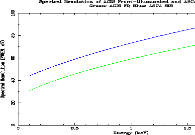
Figure 4: Comparsion of spectral resolution of ACIS front-illuminated
(FI) and ASCA SIS detectors. Both curves are derived from ground
calibration data. The ASCA data were obtained by Gendreau (MIT PhD
Thesis, 1995). ACIS FI detectors shown green; ASCA SIS detector in
blue. The ACIS curves are for ASCA grades 0,2,3,4 and 6, with
split-event threshold (spt) of 15 e ; the ASCA SIS curve is for
grades 0,2,3 and 4, for spt = 40 e
; the ASCA SIS curve is for
grades 0,2,3 and 4, for spt = 40 e . Both curves represent
pre-launch performance. Above 2 keV the FWHM curves of ACIS and ASCA
converge.
. Both curves represent
pre-launch performance. Above 2 keV the FWHM curves of ACIS and ASCA
converge.
Why do ACIS Front-illuminated detectors have better spectral resolution?
 ; ASCA uses 40 e
 .
Thus, ACIS measures smaller quantities of ``split event''charge in the
vicinity of events. This improves spectral resolution.
.
Thus, ACIS measures smaller quantities of ``split event''charge in the
vicinity of events. This improves spectral resolution.

 90 - 120 eV for E < 1.5 keV.
As we expected before the launch of ASCA, the SIS detector performance has been degraded by high-energy charged-particle radiation. A variety of measures have been taken to improve ACIS radiation tolerance. These include:
 40 pixels). ASCA experience has shown that radiation-induced
dark current varies significantly from pixel to pixel. Uncorrected,
this dark current degrades ASCA's spectral resolution. We believe the
ACIS bias map will substantially reduce the effects of
radiation-induced dark current on ACIS spectral resolution.
40 pixels). ASCA experience has shown that radiation-induced
dark current varies significantly from pixel to pixel. Uncorrected,
this dark current degrades ASCA's spectral resolution. We believe the
ACIS bias map will substantially reduce the effects of
radiation-induced dark current on ACIS spectral resolution.
 m wide;
those in ASCA devices are 3
m wide;
those in ASCA devices are 3  m wide. The narrower channels reduce
the chance that radiation-induced traps will impede the charge
transfer process.
m wide. The narrower channels reduce
the chance that radiation-induced traps will impede the charge
transfer process.
 of aluminum. This is about twice the
mean shielding carried by ASCA.
of aluminum. This is about twice the
mean shielding carried by ASCA.
The bottom line: After 5 years on orbit, (given reasonable assumptions about solar activity), we expect ACIS detector performance to be better than ASCA SIS performance was 1 year after ASCA launch.
Approach:
Results:
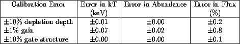
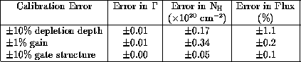
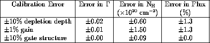
 caused the best-fit column
density to change by
caused the best-fit column
density to change by  in the power-law model with low column
density. All other parameters in the thermal and power-law models
were insensitive to errors of this magnitude in the depletion depth.
in the power-law model with low column
density. All other parameters in the thermal and power-law models
were insensitive to errors of this magnitude in the depletion depth.
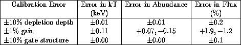
 produced peak-to-peak changes of
7--11% in the best-fit temperature for the thermal plasma models, and
had little effect on the photon index in the power law models. The
gain errors caused a change of
produced peak-to-peak changes of
7--11% in the best-fit temperature for the thermal plasma models, and
had little effect on the photon index in the power law models. The
gain errors caused a change of  in the best-fit column
density in the power-law model with low column density, and smaller
changes (
in the best-fit column
density in the power-law model with low column density, and smaller
changes ( ) in the thermal models.
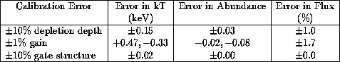
 in the thickness of the CCD gate structure (Si and
 ).
).
Conclusions:
 in the depletion depth and gate
structure, and
in the depletion depth and gate
structure, and  errors in the gain.
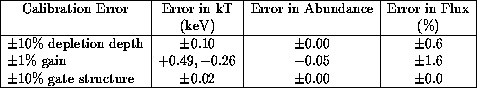
 , abund. = 0.1, Z = 0).
 , abund. = 1.0, Z = 0).
 , abund. = 0.3, Z = 0).
 , abund. = 0.3, Z = 0.5).
 ,
,  ).
).
 ,
,  ).
).